
CTIA's Tungsten Heater in Semiconductor Processing
CTIA's tungsten heater is a resistive heating element used in semiconductor manufacturing equipment to provide stable substrate heating and uniform thermal field control. The tungsten heating element is primarily applied in high-temperature processes such as wafer heat treatment, thin film deposition, epitaxial growth, and diffusion annealing, etc.
Why Choose Tungsten Heaters for Semiconductor Processing?
Stringent control over temperature windows and environmental cleanliness is essential in semiconductor fabrication. CTIA's tungsten heater meets these requirements through several key performance advantages:
(1) Structural integrity is maintained even under operating conditions approaching high-temperature limits, supporting long-cycle thermal processing.
(2) Minimal volatilization rates in vacuum and reactive atmospheres reduce chamber contamination and maintain process cleanliness.
(3) Consistent heating efficiency is preserved under continuous electrification, achieving balanced thermal field distribution through radiation.
(4) Controllable dimensional changes during repeated heating and cooling cycles help maintain process repeatability.
(5) High overall structural strength accommodates complex furnace chambers and long-term operation, minimizing the risk of deformation or failure.
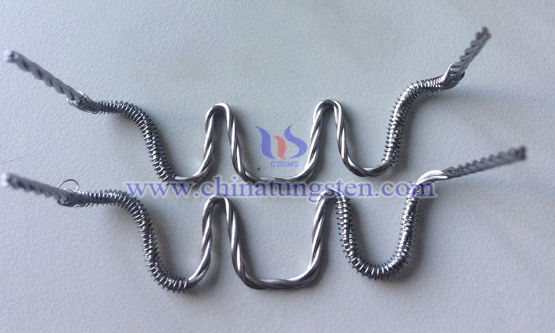
Applications of CTIA's Tungsten Heater in Semiconductor Processing
(1) Wafer Heat Treatment: Used in critical thermal processes including diffusion, annealing, and stress modulation.
(2) Thin Film Deposition: Used in Plasma Enhanced Chemical Vapor Deposition (PECVD), Physical Vapor Deposition (PVD), and Chemical Vapor Deposition (CVD) equipment for substrate heating and zone temperature management.
(3) Epitaxial Growth: Thermal support for the deposition and growth of single-crystal or compound semiconductor materials.
(4) Post-Ion Implantation: Thermal processing for lattice repair and electrical property stabilization.
(5) Research and Development: High-precision thermal support for new material characterization and micro-nano structure fabrication.
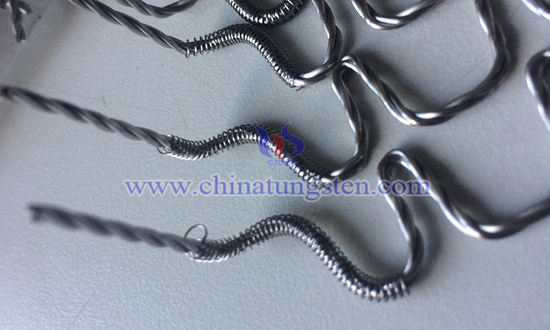
Specifications of CTIA's Tungsten Heater in Semiconductor Processing
Material: Pure tungsten wire with a purity of 99.95% or higher, or doped tungsten wire.
Wire Diameter: 0.2~1.2mm.
Strands: Single strand or multi-strand stranding.
Structure: Hump, coil, straight bar, U-frame, funnel, and customized structures.
Surface Condition: Electrolytic polishing or alkaline cleaning.
Drawing on more than 30 years of expertise in tungsten heater manufacturing, CTIA GROUP provides systematic optimization of wire diameters, doping types, structural configurations, and lead structures based on specific semiconductor chamber layouts and cleanliness standards. Combined with surface treatments such as electrolytic polishing and alkaline washing, comprehensive customized services are realized from material selection through to final fabrication.
For any inquiry, please contact?tungsten heater manufacturer: CTIA GROUP
Email: sales@chinatungsten.com
Tel: 0086 592 5129696 / 0086 592 5129595
Website: m.baixiaosheng123.com
WeChat:

More info>>
1.Tungsten heater quotation table
2. Catalog of tungsten heater
3. Tungsten heater models
4. Stranded tungsten wire for making tungsten heater