
Tungsten Crucible in Semiconductor Crystal Growth
Tungsten crucible in semiconductor crystal growth refers to the high-temperature containment component deployed in crystal growth processes for semiconductor materials including gallium arsenide, single crystal silicon, and oxides. It reliably contains high-purity melts within vacuum or inert atmospheres while providing stable thermal fields and interface control conditions for crystal growth.
Manufactured from premium high-purity tungsten (W ≥ 99.95%) through powder metallurgy sintering, hot spinning, and precision CNC machining, these tungsten crucibles are optimized for advanced semiconductor crystal growth equipment.
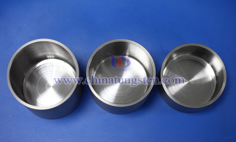
Why Select Tungsten Crucibles for Semiconductor Crystal Growth?
The semiconductor crystal growth process typically operates within thermal zones exceeding 2000°C, accompanied by prolonged thermal holding and cyclic thermal loads, which demands exceptional structural stability and purity control from the crucible material. Featuring an ultra-high melting point, extremely low vapor pressure, and excellent high-temperature creep resistance, tungsten crucibles minimize material volatilization and impurity ingress during the growth process. This enhances both crystal purity and dimensional uniformity, making them critical containment vessels in semiconductor crystal growth engineering.

Advantages of CTIA's Tungsten Crucibles in Semiconductor Growth
(1) High-Temperature Structural Stability: With melting point of approximately 3410°C, they maintain structural integrity during extended exposure to intense thermal zones.
(2) Low Vapor Pressure: Minimizes high-temperature volatilization contamination to elevate crystal purity and electrical performance.
(3) Exceptional Creep Resistance: Preserves dimensional stability under prolonged high-temperature loads, mitigating deformation risks.
(4) Thermal Field Uniformity: Facilitates the formation of stable temperature gradients to enhance crystal growth consistency.
(5) Thermal Shock Resistance: Withstands complex thermal cycling and startup/shutdown thermal impacts during the growth process.
Specifications of CTIA's Tungsten Crucibles
(1)Purity: W ≥ 99.95%
(2)Density: 17.8 ~ 18.5 g/cm3
(3)Diameter: 10 ~ 700 mm
(4)Height: 20 ~ 800 mm
(5)Wall Thickness: 1 ~ 35 mm
Tungsten crucible is primarily used in high-temperature compound semiconductor crystal growth and functional oxide material systems, encompassing crystal growth processes for materials such as gallium arsenide (GaAs), indium phosphide (InP), and zinc oxide (ZnO).
With over 30 years of deep expertise in tungsten crucible manufacturing, CTIA GROUP delivers engineered solutions optimized for semiconductor growth furnace thermal fields and specific process windows. By systematizing wall thickness uniformity, structural rigidity, and thermal matching, CTIA provide integrated solutions spanning raw material engineering to precision machining.
For any inquiry, please contact?tungsten crucible manufacturer: CTIA GROUP
Email: sales@chinatungsten.com
Tel: 0086 592 5129696 / 0086 592 5129595
Website: m.baixiaosheng123.com
WeChat:

More info>>